
Inorganic semiconductor nanostructured electrodes have a very wide range of applications in solar cells, photolysis water, and energy storage devices. The specific surface area of ​​the electrodes and the charge transport capability are the key factors that determine the performance of these devices. Recently, researcher Feng Xinjian of the Institute of Nanotechnology and Nano-Bionics of the Chinese Academy of Sciences has made a series of new developments in the research of high-performance inorganic semiconductor nano-electrodes.
The microstructure of the electrode material has an important influence on its electrical properties. The traditional electrode material with high specific surface area is formed by disorderly packing of nanoparticles. Due to the presence of a large number of grain boundaries and defects between crystal grains, the diffusion constant of charges in the crystal is lower than that in single crystal bulk materials. -8 orders of magnitude, seriously affecting the performance of the device. One-dimensional nanostructured array electrodes provide direct channels for charge transport. In the previous work, relevant persons successfully prepared a one-dimensional array of one-dimensional TiO2 nanowires on a transparent conductive glass by solvothermal method, and proved that the structure has 200 times faster electron transfer rate than the nanoparticle film by transient photoelectric test methods. (Angew. Chem. Int. Ed. 2012, 51, 2727–2730). By using the array structure electrode in a perovskite solid-state solar cell, a photoelectric conversion efficiency of nearly 12% was achieved (Chem. Comm. 2014, 50, 14720-14723. inner cover).
Array one-dimensional nanostructures possess rapid charge transport properties, but their specific surface area is much smaller than that of nanoparticle films. Therefore, nanostructures with high specific surface area and rapid charge transport properties are prepared by rationally regulating the microstructure of the electrodes. It is an important direction for the development of inorganic semiconductor nano-electrode materials in the future. Recently, researchers have prepared electrode materials that have both a high specific surface area and fast charge transport properties through two ways of regulating the microstructure.
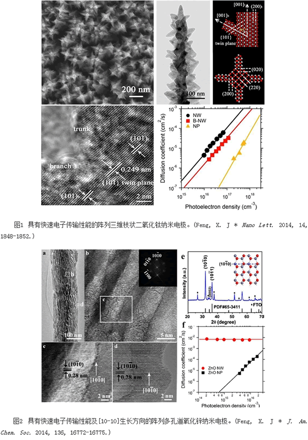
First, an array of three-dimensional branched electrode structures was prepared on the basis of an array of one-dimensional TiO2 nanowires. The branched structure is epitaxially grown along a one-dimensional trunk, which greatly reduces grain boundaries and defects between the branches and the trunk. The electrode structure has similar fast electron transport properties to the one-dimensional structure of the array, but its specific surface area is increased by 71% over the one-dimensional structure and brings about 52% improvement in the photoelectric conversion rate. Relevant work was published in Nano Lett. 2014, 14, 1848-1852, and received extensive attention, becoming the top 20 articles in the magazine with the most monthly readings.
Second, a single crystal-like array porous structure was prepared by lattice contraction of a large lattice material. By modulating the coordination dynamic process of metal ions, an array of single-crystal one-dimensional hydroxyfluoride zinc nanomaterials with a large lattice was prepared. Based on this, controllable processing was carried out, and along with the directional shrinkage of the unit cell of zinc hydroxyfluoride and the removal of small molecules, an array of porous zinc oxide nanowires with single crystal properties was obtained for the first time. This transformation also allows the prepared arrayed zinc oxide nanowires to have a special [10-10] lattice orientation. The electrode material with a thickness of 25 microns has a surface roughness factor of 955, which is comparable to a conventional nanoparticle film, and its electron transport speed is at least 1000 times faster than the nanoparticle film, and it is an ideal electrode structure. Related work was published in J. Am. Chem. Soc. 2014, 136, 16772-16775.
The above research work has received extensive attention from international counterparts. At the invitation of SPIE, he wrote a synthesis and assembly of 1D semiconductor for solar energy conversion and published it on SPIE's official website.
This series of work was supported by the national youth thousands plan, the National Natural Science Foundation of China, the Chinese Academy of Sciences and the Suzhou Nano Institute.
Manufacturing Industry Lighting
Industrial lighting is a lighting solution designed specifically for manufacturing environments. In the manufacturing industry, a good lighting solution is essential to improve production efficiency, ensure work safety and create a comfortable working environment.
Manufacturing lighting needs to meet a range of specific needs. First, there are high lighting requirements for factory lighting, because manufacturing environments often require a lot of light to ensure that employees can see details clearly when carrying out assembly, inspection, and other tasks. Second, reliability and durability are key, as manufacturing environments can have harsh conditions such as dust, vibration and high temperatures. Therefore, it is very important to use production lighting equipment with high impact resistance, dustproof, waterproof and other characteristics.
LED lighting technology has been widely used in warehouse lighting. LED lamps have the advantages of high brightness, long life, low energy consumption and low maintenance costs, which can provide efficient and reliable lighting solutions for the manufacturing industry. In addition, the intelligent control system can achieve dimming and color temperature and other functions, according to different work needs to flexibly adjust, improve energy efficiency.
Through rational planning and application of manufacturing lighting solutions, production efficiency, quality control and employee safety can be improved. Proper lighting reduces eye strain, improves accuracy, and ensures that employees can operate safely during the course of their work. The design of manufacturing lighting should consider factors such as environmental characteristics, task requirements, energy efficiency and reliability to create a safe, efficient and comfortable manufacturing environment.Manufacturing Lighting, Factory Lighting, Production Lighting, LED Lighting Technology, Warehouse Lighting
SHENZHEN LITEHOME OPTOELECTRONIC TECHNOLOGY CO., LTD. , https://www.szlitehomelight.com